- XJTAG Insights
- Posts
- Why won’t my tests work in this fixture?
Why won’t my tests work in this fixture?
Signal Integrity in Test Fixtures
Robert Humphrey - Principal Hardware & System Design Engineer
November 19, 2025
Hi reader!
Ever had a test that simply won’t run reliably – if at all – no matter what you try? Or a test that behaves perfectly on your desk, only to fall apart the moment you plug it into a fixture? You’re not alone.
Signal-integrity issues inside test fixtures and in the wiring between a Unit Under Test (UUT) and Automatic Test Equipment (ATE) are among the most common – and most often overlooked – causes of unreliable results.
The good news: a few simple design habits can make your tests dramatically more stable and reliable.
JTAG Test Access Port (TAP) signals, used to implement Boundary Scan Testing, will be used as an example, although other test and programming protocols can also benefit from following these guidelines.
Minimising the loop area
When signals are connected within a test fixture it is quite common for the wires carrying those signals to be given far more consideration than the return ground connection. A ground is likely to be included somewhere, but could it be improved?
With low frequency and DC signals, the routing of ground wires relative to the signal wires can be different without any obvious side effects. However, as the frequency of the signals increases, the routing of the ground wires becomes more and more significant, up to the point where getting matched impedances is important. For TAP signals, such levels of precision are often not necessary; however minimising the loop area is a good rule of thumb.
The key to identifying the loop area is to determine:
The route that a signal’s current will take from its source to destination. This is often easy to establish, because it is the same route as the signal’s wires and tracks.
The route that a signal’s associated return (ground) current will take from the destination back to the source. This can be slightly harder to establish, but can be approximated by assuming it stays as close to the signal as possible.
It is important to realise that this doesn’t just cover the cables between circuit boards, but also the route of the current around each board.
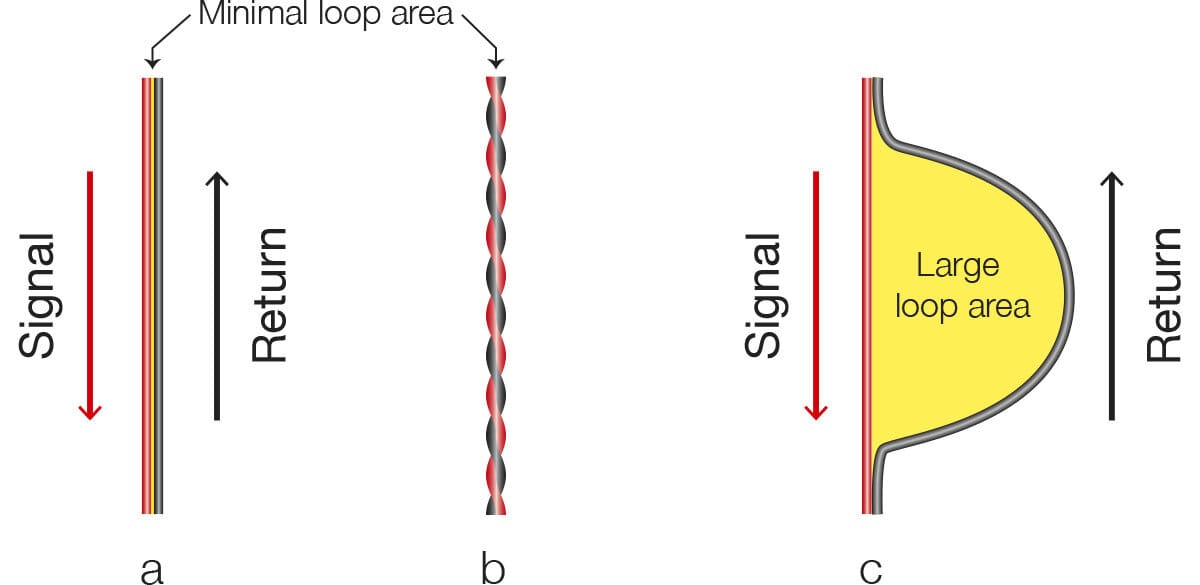
Figure 1: The arrangement of signal and return cables using (a) ribbon cables, (b) twisted pairs, and (c) individual wires, can have a significant impact on a signal’s loop area.
To minimise the loop area, the physical area bounded by the signal and its return current should be minimised. Ideally the signal and its return will be routed directly next to one another, which can be easily achieved in a ribbon cable (Figure 1a) or a traditional twisted pair (Figure 1b). Both of these arrangements have small loop areas, and so will help improve signal quality.
As soon as the return path for the ground current takes a different route to the signal current then a much larger loop area is formed causing three problems:
The signal becomes much more susceptible to Electromagnetic Interference (EMI) – the cable becomes an aerial picking up electrical noise.
The signal is radiated away from the cable, creating additional electrical noise that may interfere with other signals.
There is a change in characteristic impedance as the signal propagates down the cable. This degrades the quality of the signal.
Figure 1c shows an obvious case where there is a larger loop area, and demonstrates how easily this can occur if care is not taken to keep the signal and return wires close together.
How to minimise the loop area when creating a test fixture?
Test fixtures are often created using many individual wires, one for each active signal. Although this makes it easier to wire up the fixture, it can also lead to an electrically noisy environment and consequently signal integrity problems which are particularly evident when using JTAG.
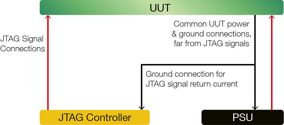
Figure 2: A bad test fixture design, due to large loop areas for all TAP signal connections.
Figure 2 shows some common mistakes seen in test fixture design: the ground connection to the JTAG controller is connected to the UUT a long way away from the TAP signal connections; and the ground and TAP signal cables do not run close to each other. This can be easily, and significantly, improved by making the following changes, as shown in Figure 3:
Add at least one ground test pin as close as possible to the TAP signal test pins in the test fixture. This isn’t for the main ground connection used to power the board, but instead is to provide a good ground connection between the JTAG Controller and the board to improve the signal quality.
Use twisted or parallel pairs, each containing one signal and a ground, for each TAP signal. This is most important for the clock signal (TCK) but also any other signals that are continuously switching (i.e. TMS, TDI and TDO). When the JTAG Controller has fixed (hard) ground pins as well as configurable (soft) ground pins, a minimum of at least one hard ground connection should be used.
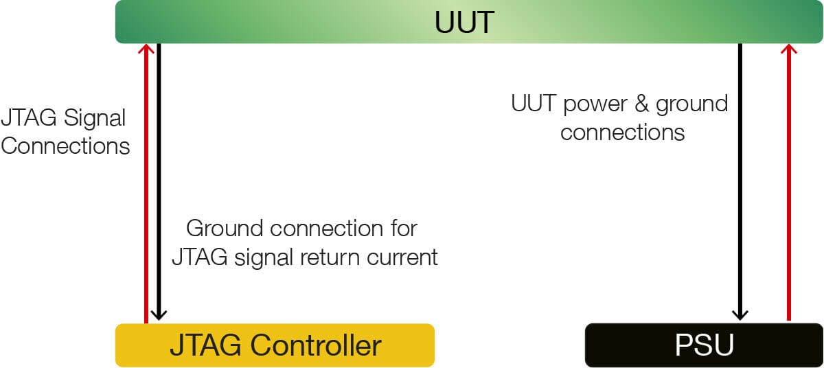
Figure 3: A good test fixture design, keeping the loop area small for all TAP signal connections.
There does not need to be a separate ground test pin for each signal/ground pair, and instead the ground cores in multiple pairs can be connected to the same test pin. If this is not directly possible then small adapter boards can be used to share one ground connection across multiple pairs. No matter how this is achieved, it is important to keep the ground and signal wires close to each other, as shown in Figure 4.
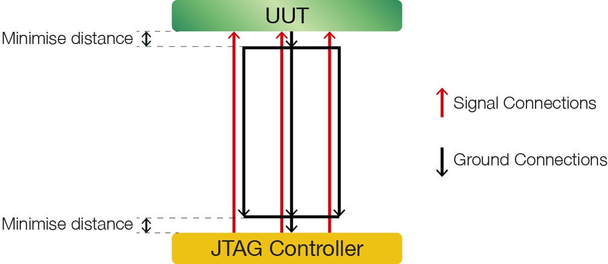
Figure 4: Wiring multiple signals when there are not enough ground connections on the UUT or JTAG Controller.
When using connectors directly on the UUT instead of test pins, a similar philosophy can still be used. For example, separating signals in a ribbon cable so they are interleaved with ground connections is sensible whenever possible, and the importance of doing this increases as the length of cables increase. If the UUT connectors are not designed to allow this organisation then it can be achieved by creating a custom cable. This might appear to be making things more complicated than they need to be; however, as previously stated, getting this right early on can significantly reduce the cost of fault finding later on during test development.
How to help minimise the loop area when designing a PCB?
To help ensure a PCB can be thoroughly and reliably tested, its testability should be considered during the design phase and not just considered as an afterthought. Design for Testability (DFT) guidelines can cover a wide range of areas, many of which focus on improving how much of a PCB can be tested. However, if the signals used to implement this testing are not considered, it is possible to design a board that can be thoroughly tested but where the tests themselves are unreliable.
Improvements to a PCB design can be split into two categories: improving signal connections to the board, and improving the signal routing within the board. The first of these should allow a test fixture to be created that can easily minimise the loop area:
When using test pins, include one ground test point close to each TAP signal test point. If board space is limited, try to include at least one ground test point for each pair of TAP signals.
When using headers that will be connected via ribbon cable, include ground pins so that there is one ground core between each TAP signal in the ribbon cable. If the number of available pins is limited, as a minimum try to include ground cores on both sides of clock signals, such as TCK.
Even with a well designed test fixture and good test signal connections to the UUT, it is still possible to make JTAG tests unreliable if a PCB is not designed correctly. Leaving the routing of the TAP signals until last might initially appear to be sensible: they’re only for testing the board, so why not route all functional signals first? The problem is that this can result in poorly routed signals that can make the testing unreliable, and in the worst case can even require a new board design, resulting in significant extra expense and delay.
It is worth keeping in mind that TAP signals can clock at frequencies exceeding 20 MHz. This means they should be treated just like any other signals at similar frequencies:
Correct signal termination should be applied to the signals, as specified in JTAG DFT guidelines. These follow standard good design practices, such as placing parallel termination resistors as near to the receiver end of a track as possible.
Avoid stubs in tracks, and use buffers to improve signal fan-out.
Route TAP signals over a continuous ground or power plane. If there are breaks in this then the loop area is increased, making the board more susceptible to unreliability during test.
Figure 5a demonstrates how the routing of a TAP signal trace (red) across a break in a ground plane can affect the return current path (black dash). This results in a larger loop area than initially expected, deteriorating the signal integrity. Although the signal track is longer in Figure 5b, the total loop area is still reduced and so this would be the preferred solution if the ground plane could not be changed.
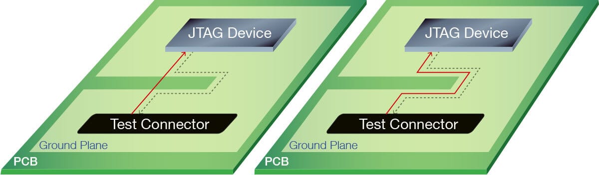
Figure 5: Return current through a ground plane (black, dashed) will follow the signal trace on a different layer (red) where possible. Routing over breaks in the ground plane (a) can significantly increase the loop area, and so should be avoided (b).
Minimising the loop area will always be a rule of thumb, and as such is not always applicable. However, by being more aware of the route a signal’s return current will take, this can provide a solid foundation when designing PCBs, determining the pin-outs for connectors, and designing and building test fixtures. By considering this as part of the design process, costly and time consuming delays later in the development cycle can be avoided.
Where available, Design for Testability (DFT) guidelines should also be consulted, because these will contain additional information to further improve the testability of UUTs and the reliability of these tests.
Design for Test (DFT) Guidelines
To further improve the reliability of your test fixtures, follow these essential tips.
Got questions or suggestions for future topics? Please get in touch and let us know.
Enjoyed this update? Please forward to a colleague who may find it interesting.