- XJTAG Insights
- Posts
- Why PCBs fail and what to do about it
Why PCBs fail and what to do about it
William Robinson - Applications Engineer
March 11, 2026
Hi reader!
Unfortunately, PCB failures are a reality. Billions of PCBs are manufactured each year, and even with robust design practices and tightly controlled assembly processes, defects are inevitable. Preventing faulty boards from reaching the market depends on understanding the underlying fault mechanisms and selecting test methods capable of detecting them. This article focuses on causes of failure in PCB production and the test methodologies used to detect them.
Modern PCB failures can be caused by a number of factors, but the most common sources of failure lie within the manufacturing process. Many of these defects are difficult or impossible to detect using visual inspection or traditional probing-based test methods, particularly on dense, BGA-heavy designs with limited physical access. Relying solely on functional testing shifts fault detection later in the development cycle, where diagnosis is slow and costly. So how can we detect these failures?
Common Failure Mechanisms
Firstly, let’s look at some common failure mechanisms introduced during the manufacturing process.
Opens
Open circuit faults (opens) are unintended breaks in the circuit that prevent current from flowing. Opens can be caused by:
| 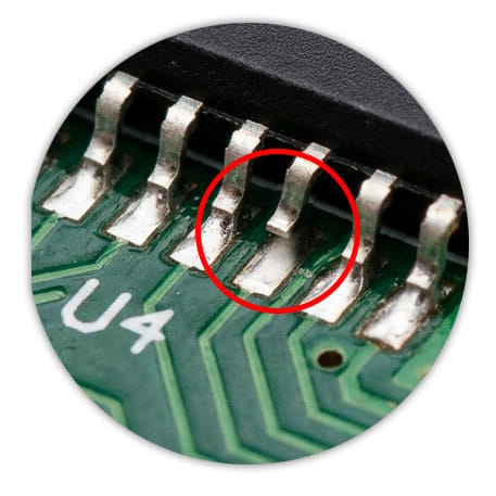 Figure 1: A lifted lead on an SMT component |
Opens are often found under BGAs due to poor solder joints if insufficient heat is applied during the reflow process to melt the BGA balls. This can be tricky to diagnose without access to a test point and may be impossible to detect using traditional test methods such as ICT (in circuit testing), AOI (automated optical inspection) or flying probe machines.
Shorts
Short circuit faults (shorts) are unintended connections between two or more areas of the circuit. Shorts can be caused by:
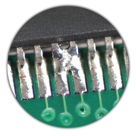 Figure 2: Solder bridge |
|
As with opens, shorts are often created under BGAs due to the difficulty of cleaning in such confined spaces. Diagnosing these shorts can be challenging due to the same lack of access discussed for open circuit detection. In many cases, the solution is simply to clean the board, perhaps using an ultrasonic cleaner, but identifying the short in the first place can still be difficult.
Components
Component-related faults are introduced during assembly as the PCB is populated. Common issues include incorrect components being fitted, such as wrong-value passive devices (for example, a 1 kΩ resistor placed where a 10 kΩ resistor is specified), incorrect variants of integrated circuits (such as a lower capacity flash memory variant of a microcontroller), or the use of counterfeit or non-qualified parts. Even when the correct component is placed in the correct footprint, assembly errors such as incorrect orientation or poor alignment can still occur and result in board failure.
Detecting Faults
Having identified several sources of manufacturing-related faults, the next challenge is detecting them as early as possible in the production process. Early detection reduces scrap, rework, and debug time, and this is achieved by applying appropriate test methodologies, some of which are outlined below.
Functional Test
One of the most widely used forms of testing, functional testing verifies that the PCB behaves as intended by exercising it in its functional or near-functional state. Power is applied and inputs are stimulated while outputs are observed, often using production firmware or dedicated test code. Functional testing validates system behaviour, but provides limited visibility into the underlying cause of a failure. |  |
Positives
| Negatives
|
In-Circuit Test (ICT)
ICT uses a bed-of-nails fixture to electrically probe individual nets and components on a powered or unpowered PCB. When physical access is available, it can measure component values, verify connectivity, and detect shorts and opens. |  |
Positives
| Negatives
|
Flying Probe Test
Flying probe testing performs ICT-style measurements using moving probes rather than a static fixture. It is typically used for prototypes and low-volume production where fixture cost is an unnecessary expense. It measures component values, verifies connectivity, and detects shorts and opens similarly to ICT fixtures. |  |
Positives
| Negatives
|
Automated Optical Inspection (AOI) and X-ray Inspection (AXI)
AOI and X-ray inspection are non-contact visual inspection techniques used to identify assembly defects during and after PCB assembly. AOI uses high-resolution cameras to detect visible issues such as poor solder paste application, missing components, orientation and alignment errors, tombstoning, and solder bridges. AXI complements AOI by imaging hidden solder joints, making it particularly effective for BGAs, QFNs, and other packages where optical access is not possible. | 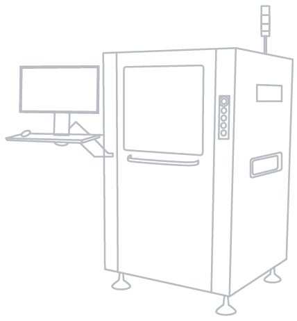 |
Positives
| Negatives
|
Boundary Scan Test
Boundary scan leverages IEEE 1149 compliant devices to control and observe I/O pins digitally via the JTAG interface. It enables testing of connections without physical probes, making it particularly effective for modern, high-density PCBs. | 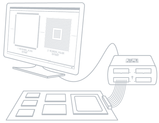 |
Positives
| Negatives
|
So, What Can We Do?
The vast majority of failed PCBs have isolated, simple faults. These problems are most likely to have been introduced during assembly due to soldering issues, or fitting incorrect components. Testing your boards immediately after assembly allows you to identify these issues before additional time, money and resources are spent on building the end product. Early testing also simplifies diagnosis; it is easier to debug a single PCB than a fully assembled product, and just reworking an individual board is far simpler than having to first extract it from a completed system.
Relying solely on functional testing of a finished product is therefore too little, too late. Instead, it’s important to implement test methodologies that can operate on individual boards, early in the process. Since different test systems have different strengths and weaknesses, the most effective approach to testing can be to combine multiple different systems, working together to maximise test coverage.
Boundary scan is an excellent starting point for early testing due to its speed, low setup cost and ability to operate without physical access. Where boundary scan coverage is limited, ICT or flying probe testing can complement it by targeting specific areas that require physical probing, while minimising the number of test points required and controlling cost. Your boundary scan and ICT systems should integrate to maximise coverage.
AOI systems also play an important role by detecting poorly formed joints that may cause early-life failures, issues that electrical tests can easily miss. Finally, functional testing remains valuable once the product is completed since it can verify full system operation, catch any issues introduced during final assembly and also allow the system to be tested at full speed.
Of course, using every available test system will catch the most issues, but this is not necessarily needed or viable. Early testing is vital, but finding an appropriate balance between coverage and cost is equally important, and boundary scan provides an excellent starting point that can offer good coverage at a very low cost.
If you would like to see what boundary scan can do for you, visit XJTAG.com to learn more about the products.
Try 5-minute Hands-on TasterUse XJTAG's tools remotely on a physical board in our lab. Follow a guided tour as you control pins, inject faults, and run diagnostics in real time. | Take a free trialTry XJTAG on your own PCBA and explore the system's diagnostic, fault-finding and in-system programming capabilities with full functionality. |
Talk to an engineerIf you’re interested and want to find out more, we’d love to talk with you. Book in a 15 minute consultation now. |
Got questions or suggestions for future topics? Please hit reply and let us know.
If you enjoyed this update, please forward to a colleague who may find it interesting.