- XJTAG Insights
- Posts
- Mission-Critical Testing
Mission-Critical Testing
Peter Fryers - Chief Operating Officer
January 14, 2026
Hi reader!
Mission-critical systems need to work, reliably and well.
To any normal reader, the unheard revolution happening in public sector secure communications may have passed you by. Countries all over the world are beginning the transition from terrestrial trunked digital radio systems such as TETRA and P25 to LTE radio such as the ESN in the UK and RRF in France. This will bring huge advantages in location and data services and will be just as transformative as the shift to digital in the 2000s.
Today a police officer can know where to go, receive critical updates and communicate seamlessly with not just the control room but other resources on the ground – all unimaginable yesterday. Tomorrow, the benefits of incorporating location services already achieved in smartphones with Advanced Mobile Location, as well as high-bandwidth data links will enable precise resource management, live video streaming and much more to keep the public safe.
With this new technology will come challenges, and the expectations for reliability and availability of mission-critical equipment only ever gets higher even as the complexity of systems grows. Not only does this equipment need to work out of the box, but it needs to keep working. This requires testing all the way up from silicon to the finished product to make sure that even the smallest intermittent or latent fault has been rooted out and corrected before it can have an impact in a mission-critical situation.
Silicon
 | An LTE radio solution will probably have at its heart a system-on-chip (SoC) such as the Samsung Exynos or Qualcomm Snapdragon families. This is a key difference from the previous generations of mission-critical electronics where chips were less capable, more application-specific and the functionality only came together at PCB level. This makes quality control at the silicon stage more valuable than ever before. Even before dicing wafers into individual chips and bonding, it is possible to contact the die test pads and identify issues. Finding faults early, especially at this stage, has two main advantages:
As well as establishing the performance of the silicon, both as a wafer, and after it is diced into individual chips, there is a whole range of testing carried out that will add value later. Verifying Memory Built-In Self Tests (BIST) and JTAG compliance at this stage are essential for the critical programming, debug and boundary scan testing stages which will come later. |
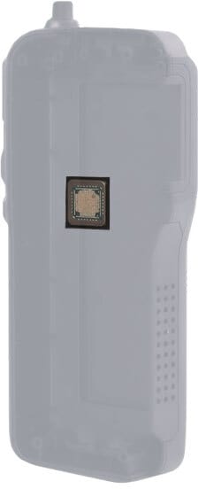
Chip
Once a SoC is packaged by wire bonding or flip-chip the silicon has a connection to the outside world. In moving from the nanometre to the micron in terms of pin density a far wider range of testing can be done to root out latent faults long before the product reaches the field. At this stage the chip manufacturer, or a silicon fab producing it under contact, will carry out a range of tests to ensure the chip will behave at the GHz speeds required using a precision test socket which can make contact with the pins in a controlled environment. These tests include measuring the electrical characteristics of the packaged chip such as voltage thresholds, clock operation and pin continuity. Also, this is the first time that radio frequency behaviours can be tested – critical for the communications functionality these systems on chip have. At this stage, if faults are found, it is very nearly impossible to make repairs and the value of the parts is still relatively low. This means that discarding rather than reworking faulty parts is normal practice here whether with the chip manufacturer or at inbound quality testing to the electronics manufacturer. |  |
Board
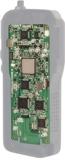 | As we reach board level, the value added to the SoC at the heart of the design increases and so the importance of finding faults, even if they don’t occur all of the time (intermittent) or have not yet developed to the stage of causing a mission-critical failure (latent), grows. Modern printed circuit board (PCB) technologies such as high-density interconnect (HDI), embedded components and blind vias allow more compact and higher speed electronics. However, they make test access ever harder, in the same way as SoCs do at the chip level. In the world of mission-critical, it is more normal to produce the electronics in-house instead of using contract electronics manufacturers because of the security requirements and valuable intellectual property in the products. This means companies need to keep significant Design-For-Test (DFT) expertise in-house. Fortunately, the functionality verified earlier now adds enormous value to the test regime. JTAG access, either through USB-enabled controllers like those made by FTDI, or brought out to a connector, allow:
|
Assembly
As the product progresses through the manufacturing process a danger emerges in designing a balanced test regime. It is possible to test too much:
The testing done at this stage is the first time that subsystems emerge that can allow end-to-end testing of specific functionality as well as allowing the testing approaches to reflect how the device will actually be used. This can involve, Human-Machine-Interface (HMI) such as keypads screens and buttons, batteries and battery management systems and the first communication to the outside world through radio frequency and LTE. The need to test all of this growing functionality leads to the risks of damage and overtesting mentioned above. | 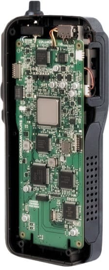 |
Product
 | Once the product is fully assembled, the cost of finding and correcting a fault has risen exponentially from the first stages of making our mission-critical product (Software Engineering Economics – Barry W. Boehm). Out there in the real world mission-critical products see harsh use and no software or electronics in the world is completely error free or 100% reliable. The End-Of-Line (EOL) testing done now is, however, the last chance to catch faults before the product is used by the customer and so will be rigorous. Faults found now will require rework which, although costly, may be preferable to throwing away an assembled product. Providing physical test access in the finished product introduces security weaknesses and so connections for diagnosis, repair and software updates will be limited. The ace-up-the-sleeve of this next generation of mission-critical communications products will be that LTE enables this to be done without a physical connection ensuring the security of the device. This test access, which in previous generations needed products to go to a repair centre, will mean that mission-critical products can be maintained and brought back into action faster and more cheaply than before – even using the very same functional and boundary scan test solutions from back in the factory. |
Testing At Every Level
More testing does not need to mean more red tape and more cost. On the contrary, testing should be effective, not just omnipresent and testing the right parts in the right places at the right time ensures that systems work when the pressure is on and costs are minimised.
With the increasing complexity of modern systems and the possibility of latent and intermittent faults hiding within, functional testing alone is not the best solution and a testing approach that spans from silicon all the way to the field ensures the best mission-critical outcomes.
Test Mission-Critical Products with Confidence
Ensure reliability, speed up diagnostics, and gain deeper insight into complex assemblies with advanced boundary-scan tools.
Take your product testing to the next level.
Got questions or suggestions for future topics? Please hit reply and let us know.
If you enjoyed this update, please forward to a colleague who may find it interesting.