- XJTAG Insights
- Posts
- Design-for-Test and Commissioning Guidelines for JTAG Test Fixtures
Design-for-Test and Commissioning Guidelines for JTAG Test Fixtures
Alan Walbridge - Senior Applications Engineer
June 18, 2025
Although many of our customers benefit from the simplicity of plugging a JTAG cable directly into a connector on their Unit Under Test (UUT), in some cases it makes more sense to use a fixturing solution to provide this connectivity. This approach can be chosen in order to reduce manual handling, reduce test time, and reduce BOM cost by removing headers.
At XJTAG, we have a lot of experience in producing and debugging these fixtures for use on high-volume production lines. The key thing to remember is that JTAG signals run at MHz frequencies, and contain frequency content at 100s of MHz and they must be taken care of accordingly.
We have included below some design-for-test and commissioning guidelines to help avoid the most common pitfalls when using a JTAG Test Fixture.
UUT Board Design
The most important step in ensuring testing connectivity is in the design of the unit to be tested. First, identify the signals that need to be managed by the JTAG controller:
TDI, TDO, TMS, TCK, as well as optional nTRST signals are required for JTAG connectivity.
For any signals referred to in the BSDL file in the “compliance” section, assess whether they will be pulled or driven to their required state on the board, and if not, allow for test points to drive them from the fixture. This can often include Power-on reset signals and mode pins.
Where possible, add XJTAG’s recommended JTAG termination to the UUT.
Next, think about how the board will be initialised. What needs to be done in order to get the board in a state where you can run boundary scan?
If power rails are normally controlled by code running in a microprocessor or CPLD, consider that this device may not be programmed at boundary scan test time, and as such this power cycle may need to be implemented using boundary scan.
Boundary scan can require additional power rails that the board doesn’t need in its mission-mode. Consider additional test points to provide power to these rails, or to allow connections to other rails of the same voltage.
If the board is part of a multi-board system, consider whether the control signals that would normally go between the boards need to be replicated using additional IO in the JTAG test fixture.
To get all of this working, think about accessing the nets on the board from the fixture – test points need to be implemented properly.
Add test points of approved diameter and spacing for all identified signals – consult your fixture provider for these values. Test points are preferable to using component pads as the component may be either mounted or not, affecting the probing requirements.
If at all possible, ensure the test points are all on one side of the board. Two-side probing entails significant additional complexity in fixture design.
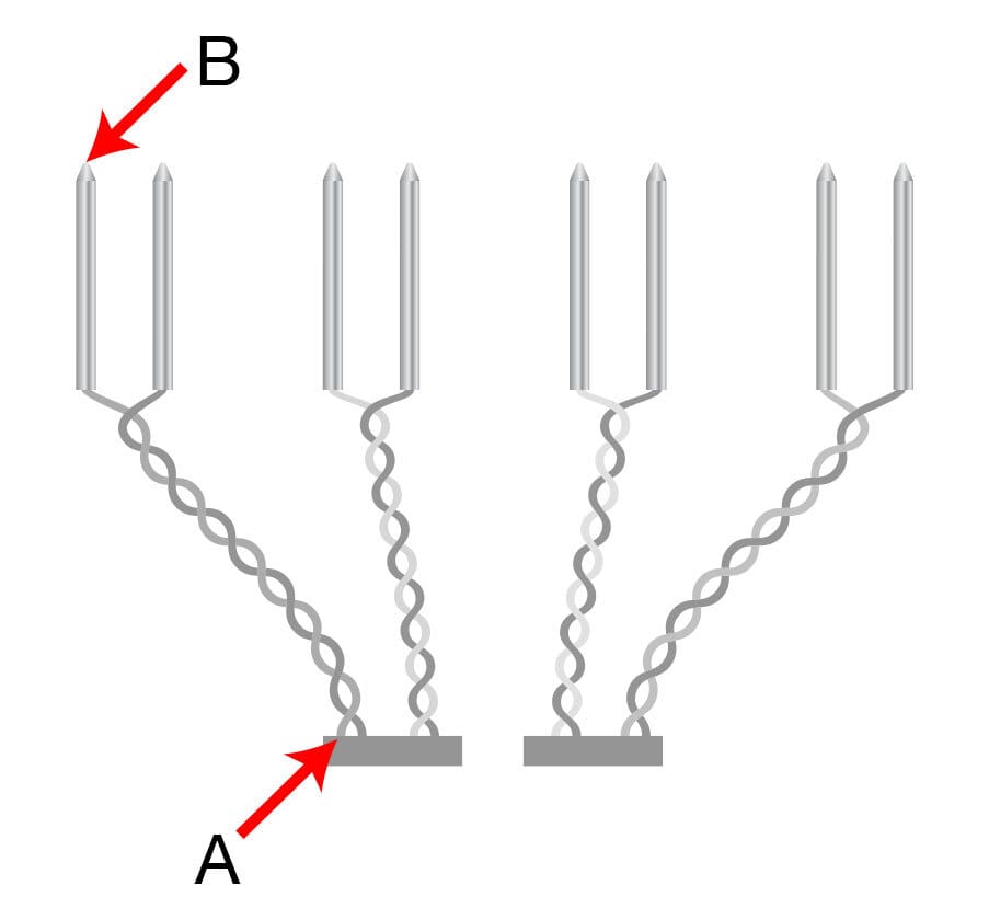
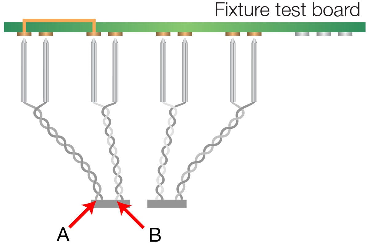
Add sufficient ground test points adjacent to the signal test points. For high-speed JTAG signals, consider adding a ground test point adjacent to each signal test point to make it easy to wire to a twisted pair. In all cases, ensure that each signal test point is less than 2-3 cm from a ground test point.
If power needs to be supplied to the board via test points, calculate the current required on these power and ground test points and ensure the test points are of sufficient size. Add additional backup ground test points in case of an open circuit.
Fixture Design
The next step is to consider the fixture that the board will be mounted in. Start off by listing all the relevant signals that will be passed from fixture to UUT:
JTAG signals
Compliance nets
Power control signals
Power supplies
For each of these signals, you will need to consider:
Logic levels (3V3, 1V8 etc.)
Signal direction
Drive type (push-pull, open-drain, etc)
Nearby grounds for all signal test points
Specify the connectivity from probes in your fixture to the controller and power supplies:
Specify a separate twisted pair from the JTAG controller and adjacent ground to the UUT and adjacent ground for each signal. Some UUT ground test points may need to be re-used – ensure that all signals are specified as twisted pairs all the way from the controller to the UUT.
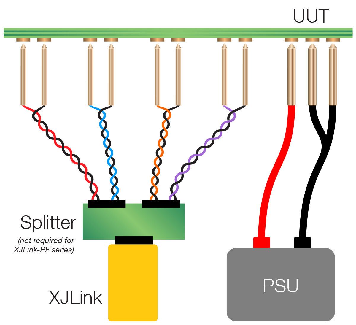
If the UUT is missing XJTAG’s recommended JTAG termination, add this to the fixture specification. Ensure that the termination is added at the UUT end, as close as possible to the test points.
Map the signals from the UUT onto the JTAG controller, ensuring that the signals are mapped to appropriate voltage banks on the JTAG controller. Using odd pins for signals and even for ground will ensure compatibility with most XJTAG hardware.
If power needs to be supplied to the board via test points, specify high-current probes to provide the power and ground directly from the UUT to the power supply. Add additional backup ground probes in case of an open circuit.
Fixture commissioning
Once the fixture is complete, it should be verified before use. Run a continuity check on every signal cable and ground cable from the JTAG controller to the tip of the probe contacting the UUT.
It is possible to use an isolation-routed PCB of the same thickness and shape as the UUT which connects pairs of pins to aid this process.
Now you can start the bring-up process by accessing the JTAG chains one-by-one and checking the signal integrity on each chain to gain confidence before moving on.
If the bring-up process finds issues with a board, we recommend the following as a starting point for debugging, in addition to the steps encountered in a normal benchtop bring-up.
No response from JTAG device at all
Check device is present on this UUT!
Check power – power sequencing code may be required either from JTAG device or directly from fixture
Check current limit on power supply
Re-check signal continuity – additionally check that UUT test points are clean
Corrupted JTAG data
Check termination is present and functional, either on UUT or on fixture
Check whether each TAP is able to run in isolation – if so there may be coupling between TAP signals due to wiring issues
Use an oscilloscope to observe the JTAG signals
If probing is required, remember that although it can be very difficult to probe a board inside a test fixture, it is often possible to solder fine wires to particular locations on the UUT before placing the board back in the fixture.
Summary
The design of both the board and the test fixture are vital to ensuring high speed, quality testing. We hope this guide has been helpful in identifying common pitfalls in designing and commissioning JTAG test fixtures. If you have any queries, or suggestions for this list, please get in touch with XJTAG directly.