- XJTAG Insights
- Posts
- Accelerating Prototype Board Bring-Up with XJTAG and Boundary Scan
Accelerating Prototype Board Bring-Up with XJTAG and Boundary Scan
Bob Storey - Chief Technology Officer
May 22, 2025
Bringing up a new prototype board typically involves thorough testing and debugging to identify design flaws, component issues, and manufacturing defects. Traditional bring-up methods, such as functional testing and manual probing, can be time-consuming and may not always provide full visibility into the board’s condition. This is where JTAG (IEEE 1149.x) and boundary scan emerge as powerful solutions for efficient and effective prototype board testing.
Prototype boards often contain faults by their very nature. As design complexity increases, identifying these faults with high confidence becomes more challenging, potentially leading to a blame game between the hardware and software engineers. This additional cost is exacerbated by higher PCB densities typically leading to lower prototype production yields and significantly higher unit costs. Therefore, employing more robust and efficient fault diagnosis equipment and processes is essential to maintaining cost-effectiveness throughout the production cycle.
Typical yield in prototype production is around 90%, however the more complex a board is, the lower this number is likely to be. Faulty boards can either be written off, adding to wastage or analysed and repaired – also a potentially costly solution.
Common Challenges in Prototype Board Bring-Up
During the early stages of a prototype’s life cycle, engineers face several challenges:
Open circuits and soldering defects – Issues such as missing, misaligned, or incorrectly soldered components can be difficult to diagnose without complete board access.
Short circuits and power faults – Identifying the root cause of power-related issues requires careful analysis, which can be hindered by complex PCB layouts.
Processor and memory bring-up – Ensuring that microcontrollers, FPGAs, and memory devices are correctly connected and functional is critical before proceeding to firmware development.
Limited physical access – As PCBs have become denser and BGAs more common, traditional bed-of-nails test fixtures struggle to provide sufficient access to all signals for in-circuit testing.
XJTAG and Boundary Scan: A Modern Solution
XJTAG and boundary scan offer a non-intrusive, systematic approach to tackling these challenges. Developed as an industry standard (IEEE 1149.1), boundary scan enables engineers to test and debug circuits, finding assembly faults without requiring physical access to every net on the PCB.
How JTAG and Boundary Scan Help in Board Bring-Up
‘Desktop’ Detection and Diagnosis of Assembly Defects
Boundary scan technology will check that the connections around the JTAG enabled devices on a board are as expected from the design and helps engineers quickly identify open and short circuits, missing components, and soldering defects by electronically probing interconnections. This helps engineers to quickly verify the integrity of critical signal paths and narrow down the faults. With XJTAG Boundary scan controllers such as the XJLink2, fault detection and diagnosis can be carried out from the desktop as a valuable and faster alternative to X-Ray inspections.
Verifying Processor and FPGA Connections
JTAG provides direct access to processors and FPGAs, allowing engineers to check if these devices are correctly powered, responding to commands, and successfully communicating with peripherals such as memory modules and I/O interfaces.
Debugging Firmware Issues
Since many modern microcontrollers and FPGAs support JTAG debugging, engineers can step through firmware execution, set breakpoints, and analyse internal registers to identify potential software or hardware interaction problems.
Automating Testing and Debugging
With XJTAG, JTAG-based testing can be automated, reducing the time required to analyse faults and ensuring consistent results across multiple prototype iterations.
Improving Efficiency and Reducing Time-to-Market
By integrating boundary scan into the prototype bring-up process, engineers can significantly reduce debugging time, enhance test coverage, and improve overall design validation. This method allows for earlier fault detection, helping to mitigate costly re-spins and ensuring a smoother transition from prototype to production.
JTAG and boundary scan are now essential tools in modern electronic design and development. Their ability to simplify the bring-up process while providing detailed insights into board functionality makes them a preferred choice for engineers worldwide.
By adopting boundary scan methodologies, companies can accelerate product development cycles, improve first-pass yields, and enhance the reliability of their designs – all while minimizing reliance on expensive physical test equipment.
Real-World Benefits of JTAG Boundary Scan with XJTAG
Many companies have successfully integrated JTAG boundary scan into their development and testing workflows using XJTAG’s solutions. Customers across almost all industries, including aerospace, automotive, consumer electronics, and telecommunication, have reported significant improvements in prototype validation, fault detection, and manufacturing test efficiency.
For example, companies developing complex, high-density PCBs have leveraged XJTAG’s boundary scan tools to detect and locate assembly defects early, reducing debugging time and eliminating the need for costly rework. By automating test routines, teams have achieved greater test coverage while reducing reliance on traditional physical probing methods.
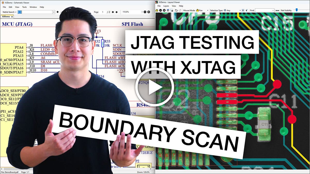
XJTAG is designed to save you time, including through the intuitive interface, the vast library of supported devices, the reusability of tests and of course bringing board testing to the engineer’s desktop. If errors are found, the built-in schematic and layout viewers will show you the exact nets or devices affected, allowing you to judge the likely causes and fix the issue, and of course by bringing your yield back towards 100%.
Manufacturers have benefited from XJTAG’s real-time diagnostics, allowing engineers to quickly isolate and resolve faults without extensive reprogramming or manual troubleshooting. This has led to faster product iterations, improved time-to-market, and overall cost savings. By adopting XJTAG’s boundary scan technology, organisations have been able to enhance product reliability, streamline development processes, and ultimately deliver higher-quality electronics to market more efficiently.
Imagination Technologies, a leader in semiconductor design, reported that XJTAG
has significantly reduced test-development effort, and we can compile effective test scripts even before the hardware is ready.
They also noted that
testing with XJTAG is our first action after the initial power-up check of a new board, and we are able to test a high proportion of each board for any manufacturing defects within around ten minutes.
Are you interested to find out more about how JTAG and XJTAG can help you with your projects? Watch this short video.